
As written in previous posts, I am busy developing an internet-enabled Nixie clock that has style. This faced me with multiple challenges such as designing a power supply, controlling the pins, and running the full assembly. A few costly PCB revisions have already been done, and it could be done way cheaper.
As the full-size PCB is 210 mm x 64 mm, it is costly to produce them in small batches with each time different revisions. 5 boards cost around 60 euros delivered, just to scrap them due to some errors. To counter this big waste of money, scaling down the PCB to verify functionality is what I went for. This is why I created an ESP32 devboard.
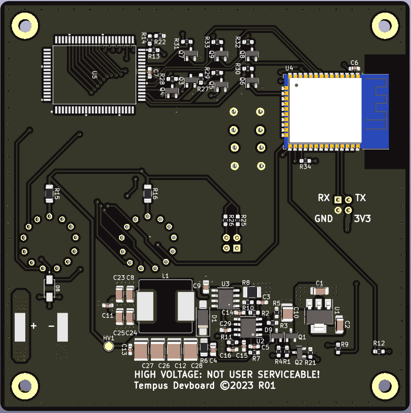
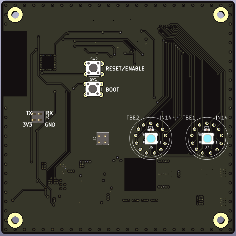
Instead of featuring 6 IN-14 tubes, it features 2 tubes and LEDs to verify their functionality. It also features buttons to figure out the programming sequence for the ESP32, as we found issues with doing this correctly.
It features basically the same power supply as designed in revision 2, with design notes seen in revision 3. This includes lower ESR input and output capacitors which are more suitable placed to decrease ripple and better diode placement to increase efficiency.
Another big mistake made in previous revisions was not taking into account the input high/low voltage of the HV57708PG which lies higher than our ESP32 can deliver. To counter this, level shifters have been added to translate 3.3 V logic to 5 V for that specific IC.
Additionally, mounting holes have been added.
The whole PCBA runs on 5V, with an exception for the UART assembly, which runs on 3.3 V.
All in all, the board size is decreased to 100 mm x 100 mm to decrease pricing in ordering. It can easily be made more compact, but since it is a development board, it is not a problem. Once the circuitry is verified to be working as it should, revision 3 of the main PCB will be released and used.
Leave a Reply